Semicon 2.0: Notification listed, chip support detailed
Approved in July 2026, Semicon 2.0 has an outlay of Rs 1,27,500 crore and separate incentives and eligibility rules for manufacturing, chip design, research and training.
In this article
Listen to this article
India Semiconductor Mission lists a gazette notification for Semicon 2.0, the programme to develop India’s semiconductor design and manufacturing ecosystem. The Union Cabinet approved the programme on 15 July 2026 with an outlay of Rs 1,27,500 crore, according to the Press Information Bureau’s 17 September explainer.
The listing concerns a scheme notified before November, rather than a newly announced Cabinet decision. KPMG’s Tax Flash News, dated 3 September 2026, identifies the Ministry of Electronics and Information Technology’s notification as F. No. W-38/6/2025-IPHW, dated 31 August 2026.
The programme extends support across chip design, manufacturing equipment and materials, fabrication plants, packaging, research and training. The Cabinet announcement published by the Prime Minister’s Office describes these as six pillars intended to build capabilities across the semiconductor industry, rather than support manufacturing plants alone.
For businesses, the distinction matters because the programme contains different routes for different activities. KPMG’s account of the notification describes capital expenditure support for manufacturing, sales-linked incentives for chip design, and project-cost support for research and talent development. These are separate categories with their own conditions, not a uniform subsidy available to every semiconductor project.
Support for factories, suppliers and chip design
According to KPMG’s September note, fiscal support for manufacturing categories ranges from 25 per cent to 40 per cent of eligible capital expenditure, meaning qualifying spending on facilities and equipment. Research and talent projects can receive support of up to 75 per cent of project cost.
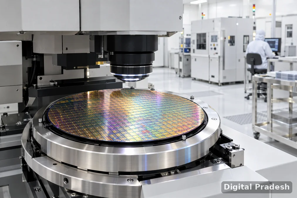
The Hindu BusinessLine reported that silicon wafer fabrication plants qualify for 40 per cent fiscal support, subject to a minimum investment of Rs 20,000 crore. A fabrication plant, or fab, processes semiconductor wafers to create the structures that make up chips, as the Press Information Bureau explains.
KPMG says capital expenditure support is disbursed on a pari-passu basis: government support accompanies qualifying project expenditure proportionately. Its account also identifies separate investment and revenue thresholds, making the size of a proposed investment only one part of the eligibility assessment.
For the machines and materials category, KPMG lists 30 per cent capital expenditure support. Minimum investment thresholds differ by activity: Rs 50 crore for raw materials, Rs 100 crore for testing and characterisation, and Rs 300 crore for equipment research and development or equipment manufacturing and assembly.
The Cabinet announcement says the machines and materials pillar will incentivise companies producing equipment, materials, chemicals and gases essential to semiconductor manufacturing. Its stated purpose is to develop the supplier base needed to sustain the industry.
Chip design has a different support structure. KPMG describes seed funding for eligible start-ups and micro, small and medium enterprises at 50 per cent of project cost or Rs 15 crore, whichever is lower. Its note also lists design infrastructure support, equity co-investment and royalty financing.
For newly launched semiconductor intellectual property, chips and system-on-chips, KPMG describes a deployment-linked incentive of 9 per cent of net sales for five years. The stated caps are Rs 30 crore per application and Rs 120 crore in aggregate per company or group. According to the note, the first launch must follow the scheme announcement, with no prior sales.
Ownership conditions also differ between design categories. KPMG says strategic design projects must be Indian-owned and controlled, while the commercial design category requires ownership and control by Indian citizens or Overseas Citizens of India. For commercial design, intellectual property and design files must remain in India, the note says.
Why the programme extends beyond fabrication
The Press Information Bureau’s explainer describes semiconductor production as a sequence involving specialised materials, wafer processing, assembly, packaging and testing. Packaging protects a chip and connects it to other electronic components; testing checks performance and quality.
This is the role of Assembly, Testing, Marking and Packaging, or ATMP, and Outsourced Semiconductor Assembly and Test, or OSAT. The Cabinet announcement says Semicon 2.0 will encourage further investment in these activities, with a focus on bringing advanced packaging technologies to India.
The same announcement identifies silicon, compound semiconductor, discrete component and display fabs as areas for further manufacturing investment. It also proposes collaboration with research centres in India and abroad to develop more advanced manufacturing processes and technologies.
The Press Information Bureau explains that a semiconductor “node” identifies a generation of manufacturing technology. Smaller node names do not, by themselves, establish better performance for every application: results also depend on design, materials and packaging. Established manufacturing processes remain important for automobiles, industrial electronics, telecommunications and power systems.
In their September 2026 report, EY and the India Electronics and Semiconductor Association argue that long-term competitiveness requires more than factory capacity. They identify reliable infrastructure, skilled personnel, research, technology commercialisation and coordination between government and industry as requirements for developing competitive semiconductor clusters.
Existing projects and application scrutiny
Semicon 2.0 follows the first programme, approved in December 2021 with an outlay of Rs 76,000 crore, according to the Press Information Bureau. That programme supported semiconductor and display fabrication, other semiconductor manufacturing activities, packaging and chip design.
In its 17 September account, the bureau reported 12 approved manufacturing units carrying cumulative investment of more than Rs 1.64 lakh crore. It listed their locations as Gujarat, Assam, Uttar Pradesh, Odisha, Punjab and Andhra Pradesh, and said five units had commenced commercial production. Those figures describe the position reported in September, not a November production update.
KPMG’s account places India Semiconductor Mission at the centre of the application process. It says the mission assesses proposals on technical and financial parameters, including process technology, implementation capacity, operating capability and arrangements for selling output, before forwarding recommendations to the ministry.
According to KPMG, design and talent projects follow an approval structure based on project cost: the ministry’s secretary handles projects below Rs 100 crore, the minister handles projects from Rs 100 crore to Rs 500 crore, and the Union Cabinet handles those above Rs 500 crore. Other categories require Cabinet approval.
The September note describes an initial three-year application window through the mission’s portal and a mid-term appraisal after three years of implementation. It says project duration is preferably up to six years, to be decided project by project. It also records that category-specific guidelines, requests for proposals for strategic design, and separate research and talent guidelines were to be issued separately.

Please log in to leave a comment.


